Brand logo

MICROELECTRONICS & OPTOELECTRONICS

Applications

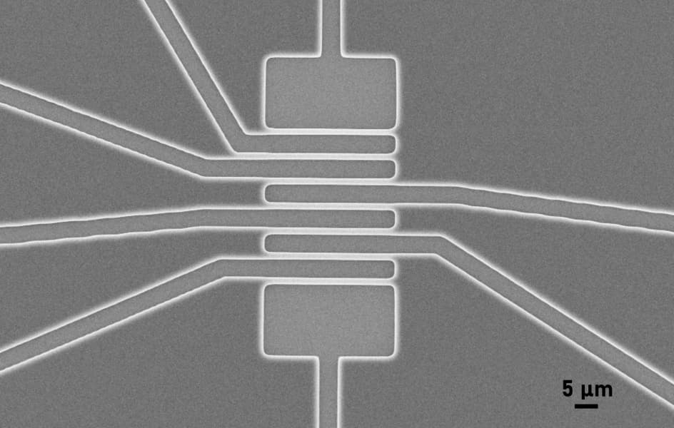
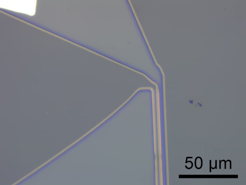
Contact electrodes patterned in a AZ 1512 HS resist before metal deposition - Realized with Smart Print UV

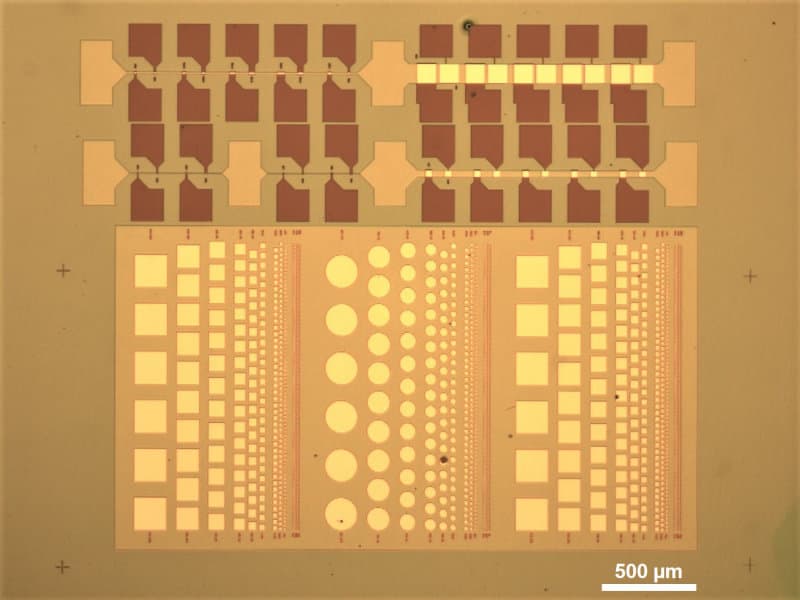
Device with realignment step on the tracks to define electrodes in the resist (top of the image) and definition of junctions (square and round) in the resist (bottom of the image) – Courtesy of F. Godel, France - Realized with Smart Print UV

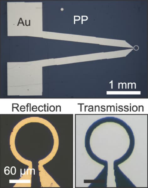
Microheater actuator on a PolyPropylene substrate for straintronic applications - Courtesy of A. Castellanos-Gomez, Spain, Nano Lett. 2020, 20, 5339−5345 - Realized with Smart Print UV

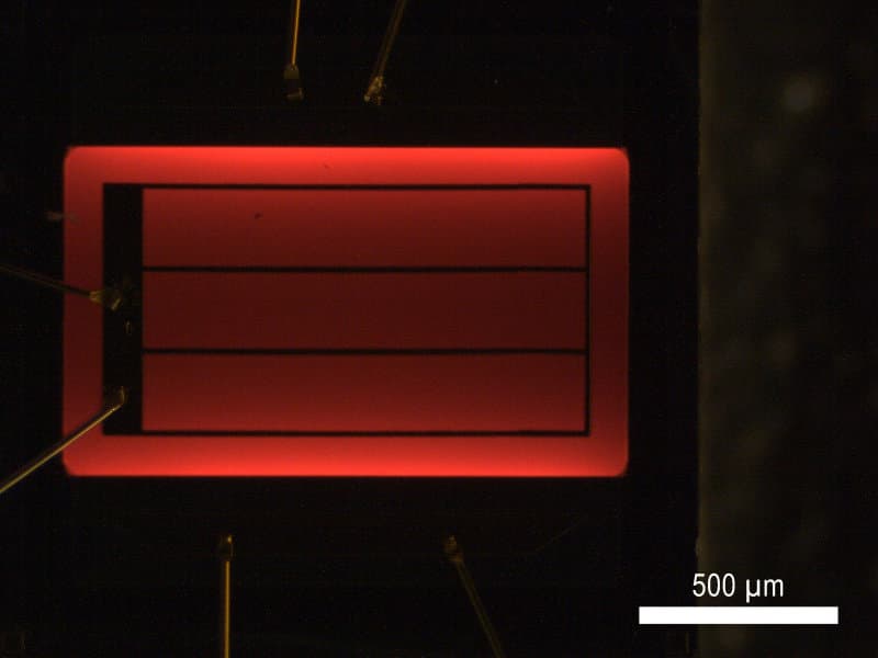
GaInP solar cell structures, Courtesy of E. Antolin, Spain - Realized with Smart Print UV

Undercut structure fabricated on a bilayer resist on a sapphire substrate - Courtesy of E. Antolin, Spain - Realized with Smart Print UV

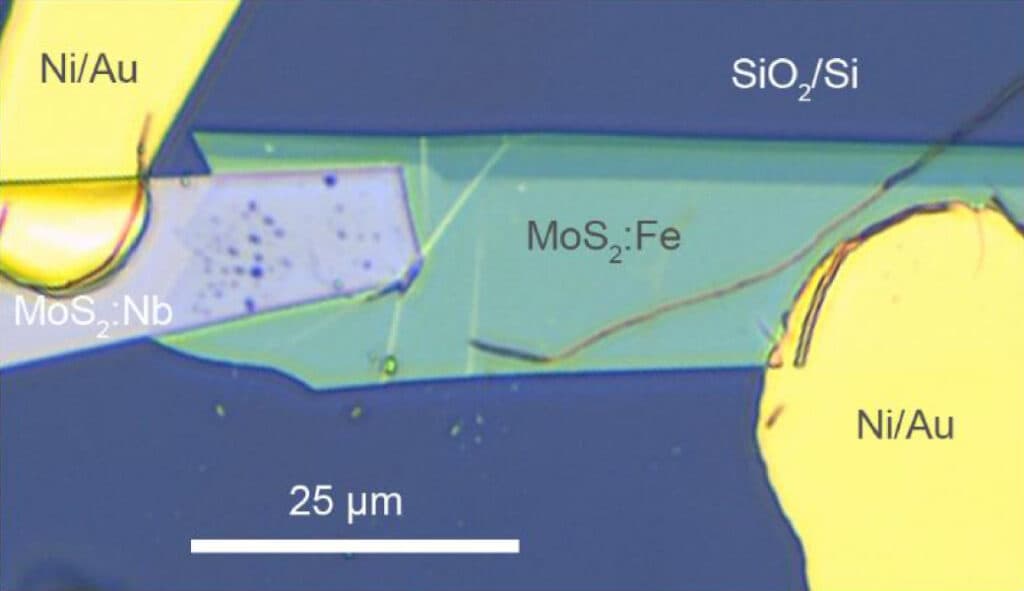
MoS2 van der Waals homojunction solar cell on SiO2/Si - Courtesy of E. Antolin, Spain, Nano Energy, 2021, 79, 105427 - Realized with Smart Print UV

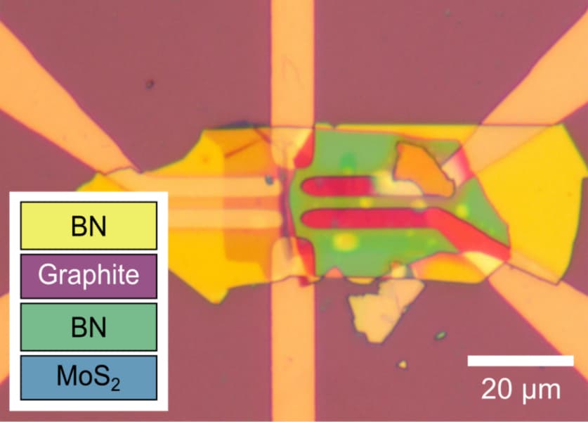
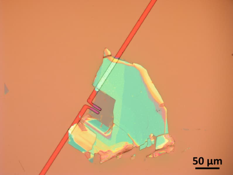
FET devices based on Graphene and MoS2 flakes – Courtesy of J. Island, USA, Nanomanufacturing 2021, 1, 49–56 - Realized with Smart Print UV

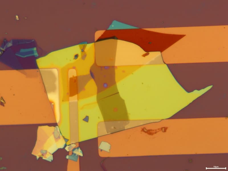
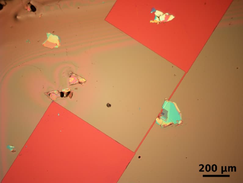
Exfoliated 2D materials transferred on contact electrodes – Courtesy of J. Island, USA - Realized with Smart Print UV

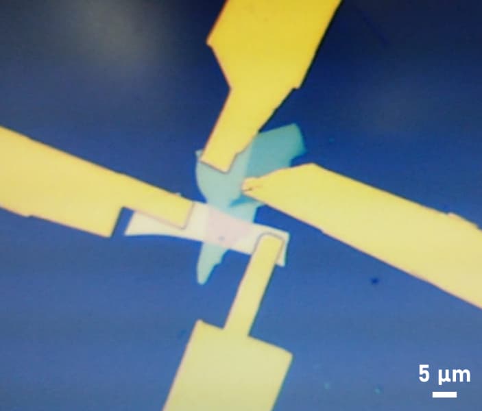
Contact electrodes on GaSe 2D flakes – Courtesy of A. Castellanos-Gomez, Spain - Realized with Smart Print UV

Contact electrodes on GaSe 2D flakes – Courtesy of A. Castellanos-Gomez, Spain - Realized with Smart Print UV

Contact electrodes on exfoliated 2D materials – Courtesy of E. Antolin, Spain - Realized with Smart Print UV

manage cookies consent
Microelectronics & Optoelectronics - Microlight3D