2D MATERIALS
Applications
Smart Print UV allows for the direct exposure of a digital design without the need of a traditional photomask. It is therefore perfectly suited for rapid prototyping and custom fabrication of microstructures such as contact electrodes for 2D materials research with very high precision.
One of the key features of SP-UV is its precise alignment capability, displaying the design on the substrate in real time, allowing direct printing on already structured surfaces. Equipped with a 385 nm UV light source, Smart Print UV is compatible with photoresists dedicated to etching and lift-off processes (AZ1500, AR-P 5300, S 1800 series ...).
This alignment function also enables the creation of multi-layer material-on-material architectures, for example to deposit photopolymerizable resins on 2D materials without degrading them, or to create functional microstructures precisely positioned relative to sensitive layers.
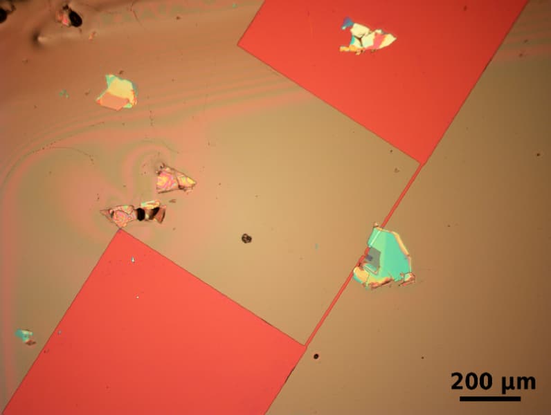
Contact electrodes on GaSe 2D flakes – Courtesy of A. Castellanos-Gomez, Spain - Realized with Smart Print UV
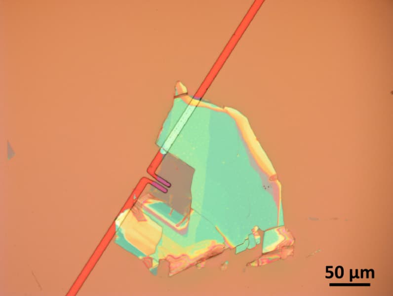
Contact electrodes on GaSe 2D flakes – Courtesy of A. Castellanos-Gomez, Spain - Realized with Smart Print UV
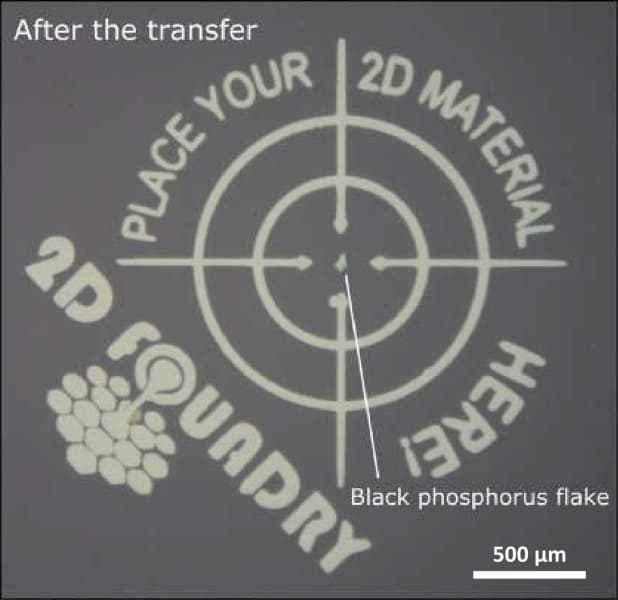
Crosshair markers for deterministic transfer of 2D flakes (black phosphorus) – Courtesy of A. Castellanos-Gomez, Spain, Nano Lett. 2020, 20, 5339−5345 - Realized with Smart Print UV
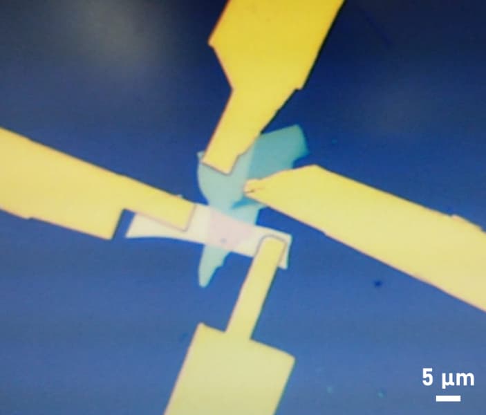
Contact electrodes on exfoliated 2D materials – Courtesy of E. Antolin, Spain - Realized with Smart Print UV
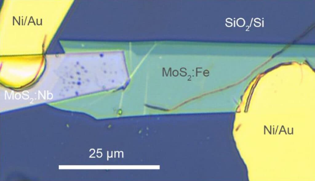
MoS2 van der Waals homojunction solar cell on SiO2/Si - Courtesy of E. Antolin, Spain, Nano Energy, 2021, 79, 105427 - Realized with Smart Print UV
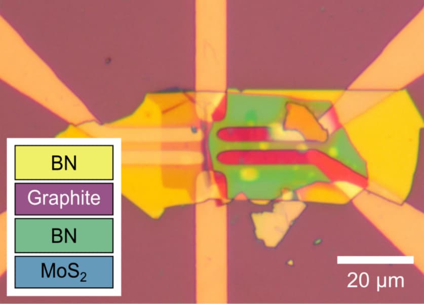
FET devices based on Graphene and MoS2 flakes – Courtesy of J. Island, USA, Nanomanufacturing 2021, 1, 49–56 - Realized with Smart Print UV
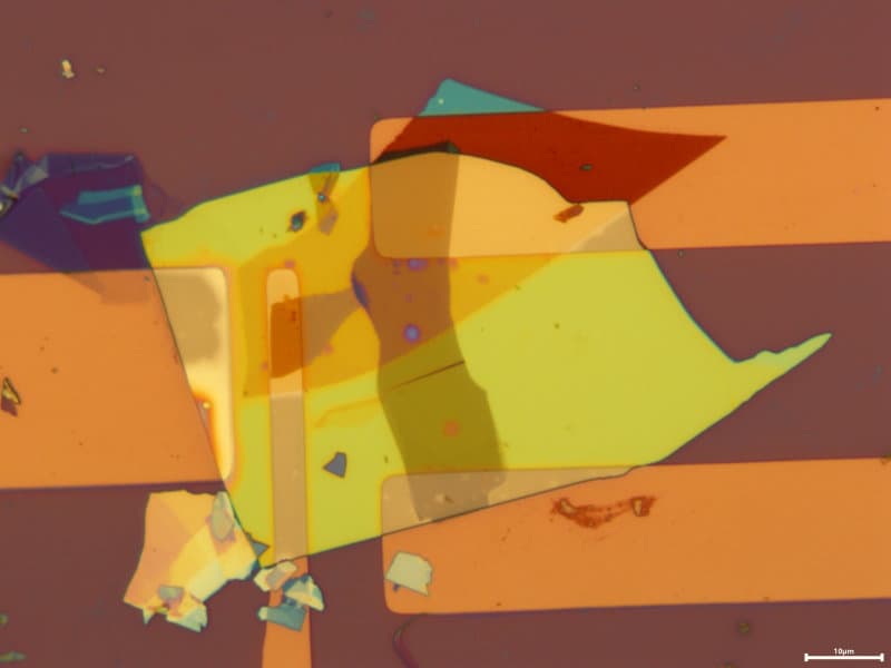
Exfoliated 2D materials transferred on contact electrodes – Courtesy of J. Island, USA - Realized with Smart Print UV